Quick Start
This board needs no library and no code of its own. It sits in the signal path between a higher-voltage system and a lower-voltage one, so you keep using the code you already have for your device. The example below joins a 5 V controller and a 3.3 V I2C device.
1. Connect the breakout board
Solder the included header pins first if you want to use the board on a breadboard. Then power each side from its own system and wire the signals:
| Your boards | Logic Level Converter I2C TXS0104 Breakout |
|---|---|
5 V controller, 5V | VCCH |
5 V controller, GND | GND (right header) |
5 V controller, SDA | B1 |
5 V controller, SCL | B2 |
3.3 V device, 3V3 | VCCL |
3.3 V device, GND | GND (left header) |
3.3 V device, SDA | A1 |
3.3 V device, SCL | A2 |
Each A pin is paired with the B pin of the same number, so any two channels
work for SDA and SCL. Leave OE unconnected: a 10 kΩ resistor on the board
holds it high, which keeps the outputs on.
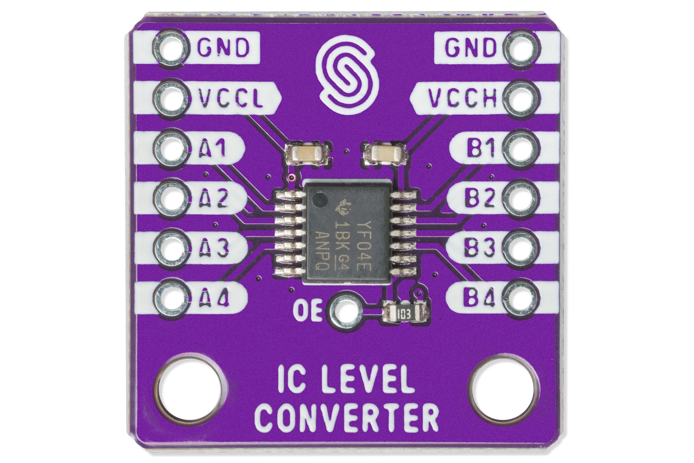
VCCL must never be higher than VCCH. Put the lower supply (1.65 V to 3.6 V)
on VCCL and the higher one (2.3 V to 5 V) on VCCH. Equal supplies, such as
3.3 V on both sides, are fine.
2. Check the result
Run the sketch or program you normally use for your device. The controller now talks to it through the board as if the two were wired together directly. The board adds no I2C device of its own, so an I2C scan lists only your device, at its usual address.
3. If it does not work
Continue with Troubleshooting and retry after each change.