Hardware Details
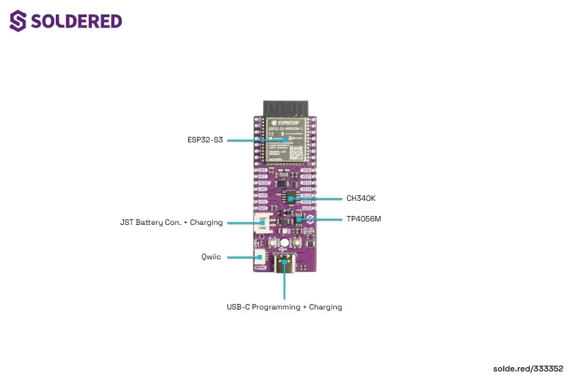
NULA DeepSleep ESP32-S3 breaks out the ESP32-S3's GPIO pins on two rows of breadboard-compatible header holes, with power, reset and UART pins alongside. A Qwiic connector carries power and I2C (a two-wire bus for talking to chips) on one cable, so you can add a sensor without using header pins. The board also has a JST battery connector with an onboard charger, a PCF85063A real-time clock, a CH340K USB-to-serial chip, a USER button, a RESET button and an addressable RGB LED on IO2.
Pinout

Pin details
| Pin marking | Pin name | Description |
|---|---|---|
| RXD | RXD0 | UART receive (GPIO44) |
| TXD | TXD0 | UART transmit (GPIO43) |
| 13 | IO13 | Digital I/O, SPI MISO (FSPI MISO), ADC input, PWM |
| 11 | IO11 | Digital I/O, SPI MOSI (FSPI MOSI), ADC input, PWM |
| 12 | IO12 | Digital I/O, SPI clock (FSPI CLK), ADC input, PWM |
| 10 | IO10 | Digital I/O, SPI chip select (FSPI CS), ADC input, PWM |
| 4 | IO4 | Digital I/O, ADC input, PWM |
| 5 | IO5 | Digital I/O, ADC input, PWM |
| IO6 | IO6 | Digital I/O, ADC input, PWM |
| IO7 | IO7 | Digital I/O, ADC input, PWM |
| RESET | RESET | Control pin, resets the board |
| 3V3 | 3V3 | Power supply pin, 3.3 V |
| GND (left row) | Ground | Ground reference |
| VCC | VCC | Power supply pin |
| BAT | BAT | Power supply pin, battery |
| 8 | IO8 | Digital I/O, I2C data (SDA), ADC input, PWM |
| 9 | IO9 | Digital I/O, I2C clock (SCL), ADC input, PWM |
| 42 | IO42 | Digital I/O, PWM |
| 41 | IO41 | Digital I/O, PWM |
| 40 | IO40 | Digital I/O, PWM |
| 39 | IO39 | Digital I/O, PWM |
| 38 | IO38 | Digital I/O, PWM |
| 0 | IO0 | Digital I/O, strapping pin (it sets the boot mode at reset), also wired to the USER button |
| IO48 | IO48 | Digital I/O, PWM |
| IO47 | IO47 | Digital I/O, PWM |
| IO21 | IO21 | Digital I/O, PWM |
| IO14 | IO14 | Digital I/O, ADC input, PWM |
| IO19 | IO19 | Digital I/O, ADC input, PWM |
| IO20 | IO20 | Digital I/O, ADC input, PWM |
| GND (right row) | Ground | Ground reference |
Some GPIOs are not on a header. IO2 drives the onboard WS2812B RGB LED, and IO17 receives the real-time clock's interrupt output. The USER button pulls IO0 low and the RESET button pulls EN low. Three small LEDs show activity: red for charging (CHRG), blue for TXD0 and white for RXD0.
Power supply
Power the board over USB-C, which also programs it through the CH340K. A 500 mA fuse protects the USB input. For battery projects, plug a Li-Ion or Li-Po battery into the 2-pin JST connector. The onboard TP4056M charger charges it from USB, and the board picks USB or the battery as its power source on its own. A TPS7A2633 regulator makes the 3.3 V rail, and the board's logic is 3.3 V. Check the battery connector's polarity against the marking on the board before you plug a battery in. The charging current is set by a 3 kΩ resistor on the charger's PROG pin, which gives about 400 mA.
Real-time clock and I2C
The PCF85063A real-time clock (RTC) sits on the same I2C bus as the Qwiic connector, at address 0x51. A 32.768 kHz crystal keeps its time. The bus has 4.7 kΩ pull-up resistors to 3.3 V on SDA and SCL, so a Qwiic sensor needs none of its own.
Dimensions
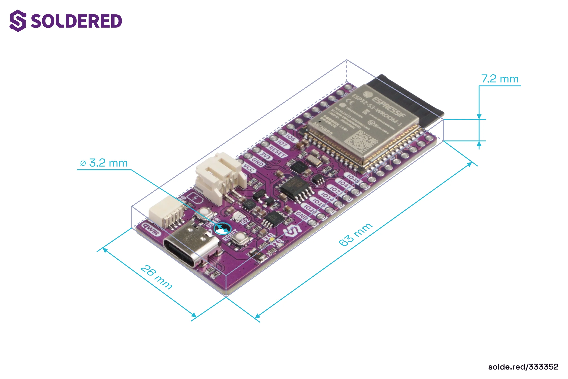
- Board size: 63 × 26 mm, 7.2 mm high
- Header spacing: the two header rows are 22.86 mm (0.9 in) apart, so the board is breadboard-compatible. Header pins are included but unsoldered.
- Mounting: one 3.2 mm diameter mounting hole, between the USER and RESET buttons
Jumpers
| Jumper | Default | Function |
|---|---|---|
| JP1 | Connected (NC, normally closed) | Cut to disconnect the WS2812B RGB LED from VCC |
With JP1 cut, the onboard LED stays dark and the Quick Start Blink example shows nothing.