Hardware Details
The board carries the Bosch BMM350 magnetometer, a 1.8 V regulator, an I2C level shifter, two Qwiic connectors, a 4-pin and a 2-pin 2.54 mm header, and five solder jumpers.
Key specifications
| Specification | Value |
|---|---|
| Interface | |
| Interface | I2C; INT data-ready output |
| Qwiic compatible | Yes, 2x Qwiic connector |
| Default I2C address | 0x14 |
| I2C address changeable | Yes, 0x15 with jumper JP5 |
| Breadboard compatible | Yes, 4-pin and 2-pin 2.54 mm headers (supplied unsoldered) |
| Measurement | |
| Measurement types | Magnetic field, 3 axes; sensor temperature |
| Measurement range | ±2000 µT on all axes; output data rate 25/16 Hz to 400 Hz in normal mode, without averaging at 400 Hz (the libraries start at 100 Hz with 4-sample averaging, and lower it to 2 samples at 200 Hz and to none at 400 Hz); forced mode up to 200 Hz, without averaging only |
| Measurement accuracy | Resolution about 0.1 µT; zero-field offset ±25 µT typical (25 °C), ±2 µT typical after Bosch eCompass calibration; sensitivity error ±1 % (X, Y), ±3 % (Z) typical |
| Power | |
| Supply voltage | 2 V to 5 V on the header 3V3 pin; the Qwiic connectors share that supply |
| Logic level | SDA, SCL: level-shifted, same as the supply; INT, AD: 1.8 V |
| Operating current | 350 µA typical, normal mode, 100 Hz, 4-sample averaging, the setting both libraries start in (200 µA with 2-sample averaging) |
| Suspend current | 1.8 µA typical |
| Other | |
| IC part number | Bosch BMM350 |
| Operating temperature | -40 to +85 °C |
| Dimensions | 22 x 22 mm |
| Mounting holes | 2x 3.2 mm |
The current figures are the BMM350's typical values for the sensor alone. The normal-mode figures are given at 25 °C; the suspend figure is given with no temperature.
Pinout
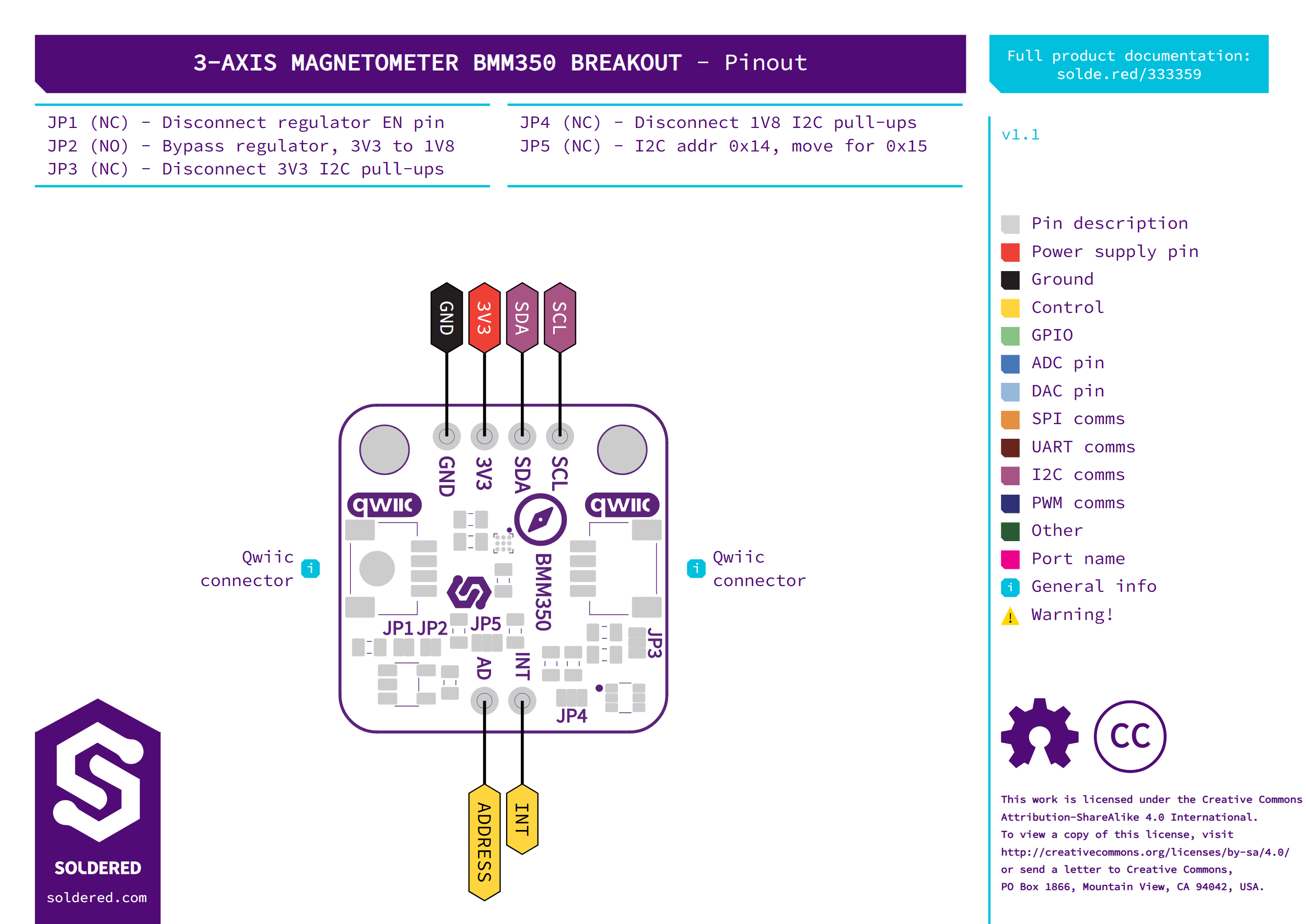
| Pin marking | Pin name | Description |
|---|---|---|
GND | Ground | Ground, shared with both Qwiic connectors. |
3V3 | Supply | 2 V to 5 V supply for the board's regulator and level shifter, shared with both Qwiic connectors. |
SDA | I2C data | I2C data line, level-shifted to the supply on 3V3. |
SCL | I2C clock | I2C clock line, level-shifted to the supply on 3V3. |
AD | Address | The BMM350's address pin, straight from the sensor at 1.8 V logic: low selects 0x14, high selects 0x15. Set by JP5 (see Jumpers). |
INT | Interrupt | The BMM350's data-ready interrupt output, straight from the sensor at 1.8 V logic. |
Voltage and logic levels
| Connection | Supported voltage | Notes |
|---|---|---|
3V3 pin | 2 V to 5 V | Feeds the onboard 1.8 V regulator and the I2C level shifter. |
| Qwiic connectors | Same as 3V3 (2 V to 5 V) | On the same supply net as the 3V3 pin. |
SDA, SCL | Same as 3V3 | Through the I2C level shifter. |
INT, AD | 1.8 V | No level shifter on these pins. |
The Qwiic connectors are on the same supply as the header. When you power
the 3V3 pin from 5 V, both Qwiic connectors carry 5 V too, so do not chain
3.3 V-only Qwiic boards from this breakout then.
INT is a 1.8 V signal. The controller pin you connect it to has to read
1.8 V as a logic high.
Dimensions
The board is 22 x 22 mm with two 3.2 mm mounting holes. The headers use the standard 2.54 mm pitch.
Jumpers
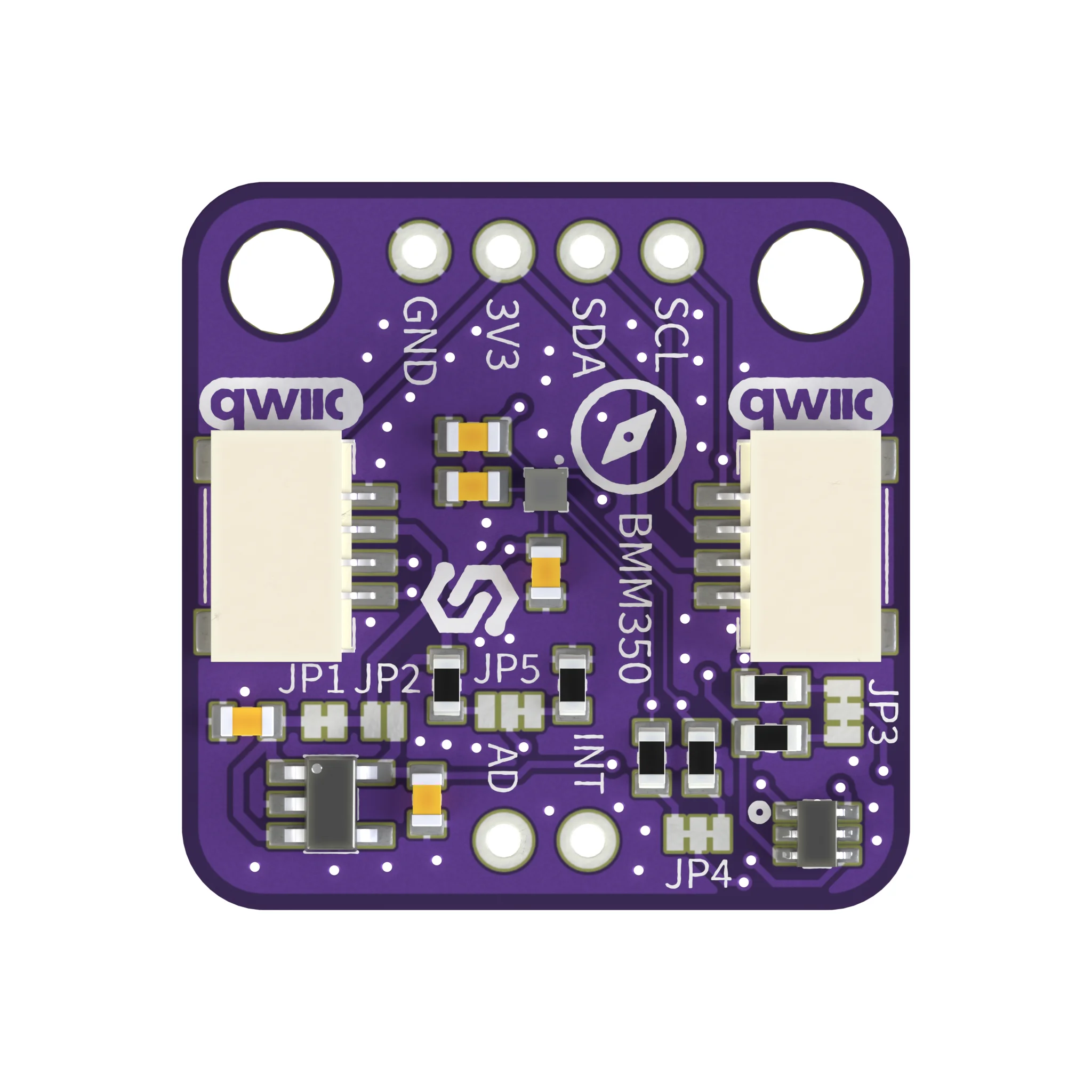
The jumpers are labelled on the board. With the GND, 3V3, SDA, SCL
header at the top, as in the photo, JP1 and JP2 sit at the lower left,
under the left Qwiic connector. JP5 sits in the middle, above the AD and
INT pins. JP3 sits at the right, under the right Qwiic connector, and JP4
at the bottom right.
| Jumper | Default | Function |
|---|---|---|
JP5, address | Closed: address 0x14 | Move it for 0x15: cut the default side and bridge the other side with solder. |
JP3 and JP4, I2C pull-ups | Closed: pull-ups connected | JP3 disconnects the I2C pull-ups on the 3V3 side, JP4 the ones on the 1.8 V side. Cut a jumper to disconnect its pull-ups. |
JP1, regulator enable | Closed | Cut it to disconnect the regulator's enable pin. |
JP2, regulator bypass | Open | Bridge it to bypass the regulator, connecting 3V3 to the 1.8 V side. |
Never leave the address pin floating: the BMM350 needs a defined level on it,
or its I2C address is undefined. If you cut JP5's default side, bridge the
other side.
Leave JP2 open unless you feed the board 1.8 V. Bridging it puts the
voltage on 3V3 straight onto the 1.8 V side. The BMM350 runs from 1.72 V to
1.98 V, and 2 V is its absolute maximum supply.
Hardware repository
The hardware repository for this board is not available yet! We are working on it. In the meantime, please contact us to receive the hardware files.