Hardware Details
The breakout has a USB-C connector, a CP2102N USB to UART bridge and an SE5218 3.3 V regulator. A 500 mA fuse protects the USB 5 V line. The 6-pin FTDI header sits on the right edge, with a 6-pin header on the top edge and an 8-pin header on the bottom edge.
Key specifications
| Specification | Value |
|---|---|
| Interface | |
| Interface | UART, USB |
| USB | USB-C, USB 2.0 Full Speed |
| Baud rate | Up to 3 Mbaud |
| UART lines | TXD, RXD, RTS, CTS, DTR, DSR, DCD, RI |
| Other pins | GPIO0 to GPIO3, SUSP, SUSPb |
| Qwiic compatible | No |
| Breadboard compatible | Yes |
| Power | |
| Supply voltage | 5 V, from the USB-C connector |
| Logic level | 3.3 V only |
| VCC pin output | 5 V or 3.3 V, set with a slide switch |
| 3.3 V regulator | SE5218 |
| Max output current | 0.5 A |
| Protection | Overcurrent, 500 mA fuse on the USB 5 V line |
| Other | |
| IC part number | CP2102N-A02-GQFN24 (Silicon Labs) |
| Dimensions | 38 × 22 mm |
| Mounting holes | 2 × 3.2 mm |
| LEDs | TX, RX and PWR |
Pinout
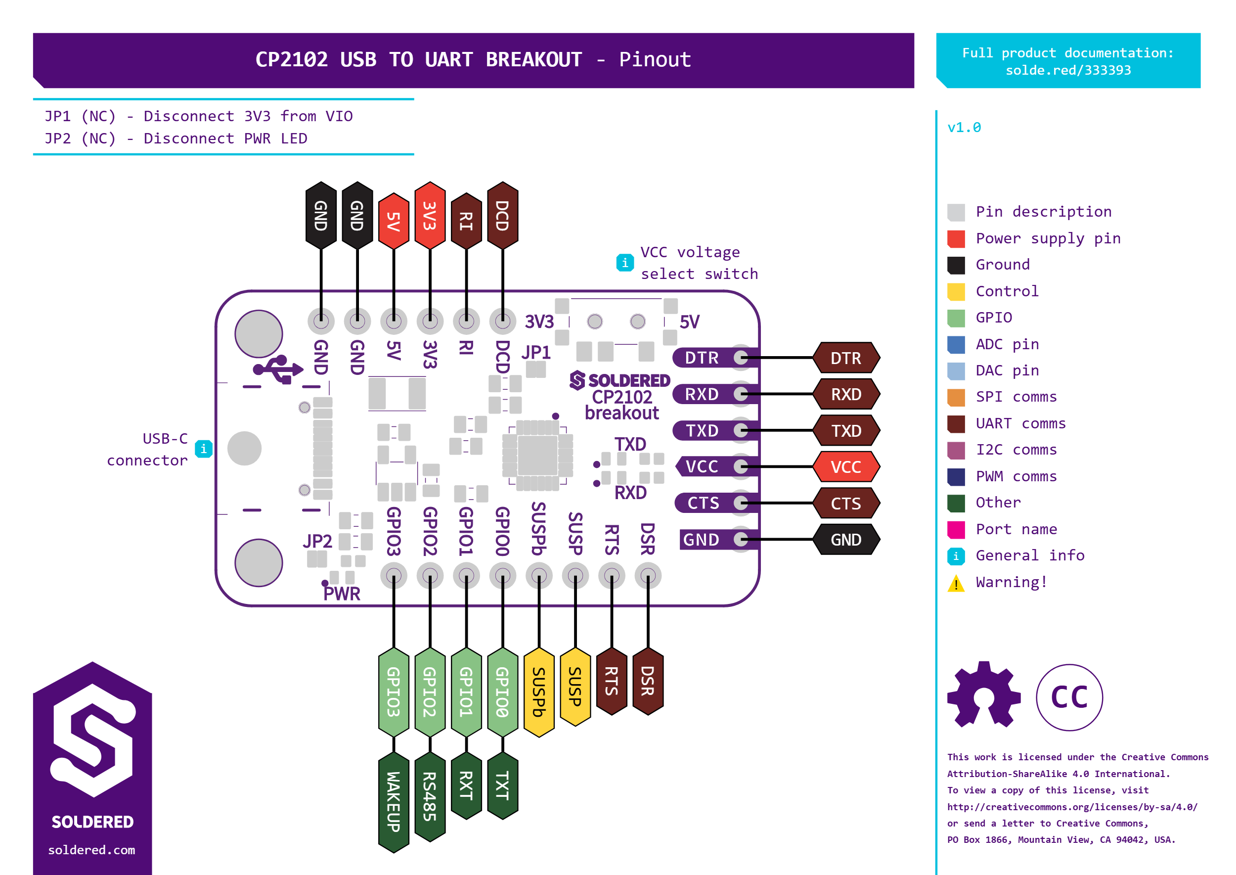
FTDI header (right edge), from the top of the pinout drawing:
| Pin marking | Pin name | Description |
|---|---|---|
| DTR | DTR | Data Terminal Ready. Resets boards such as the Arduino Pro Mini before an upload. |
| RXD | RXD | Receives data. Connect it to the TX pin of your board. |
| TXD | TXD | Sends data. Connect it to the RX pin of your board. |
| VCC | VCC | Power for the board you connect. 5 V or 3.3 V, set with the slide switch. |
| CTS | CTS | Clear To Send. |
| GND | GND | Ground. |
Top header (6 pins), left to right in the pinout drawing:
| Pin marking | Pin name | Description |
|---|---|---|
| GND | GND | Ground. |
| GND | GND | Ground. |
| 5V | 5V | 5 V from the USB-C connector, after the fuse. |
| 3V3 | 3V3 | 3.3 V from the on-board regulator. |
| RI | RI | Ring Indicator. |
| DCD | DCD | Data Carrier Detect. |
Bottom header (8 pins), left to right in the pinout drawing:
| Pin marking | Pin name | Description |
|---|---|---|
| GPIO3 | GPIO3 | General-purpose pin. Alternate function marked WAKEUP. |
| GPIO2 | GPIO2 | General-purpose pin. Alternate function marked RS485. |
| GPIO1 | GPIO1 | General-purpose pin. Alternate function marked RXT. |
| GPIO0 | GPIO0 | General-purpose pin. Alternate function marked TXT. |
| SUSPb | SUSPb | Suspend output, the active-low version of SUSP. |
| SUSP | SUSP | Suspend output. |
| RTS | RTS | Request To Send. |
| DSR | DSR | Data Set Ready. |
Voltage and logic levels
| Connection | Supported voltage | Notes |
|---|---|---|
| USB-C | 5 V | Powers the board through a 500 mA fuse. |
| TXD and RXD | 3.3 V logic | The switch does not change the logic level. |
| VCC pin on the FTDI header | 5 V or 3.3 V | Set with the VCC voltage select switch. |
| 5V pin on the top header | 5 V | Follows the USB-C supply, not the switch. |
| 3V3 pin on the top header | 3.3 V | From the SE5218 regulator. |
Note. The slide switch changes only the voltage on the VCC pin. The UART pins stay at 3.3 V logic in both positions.
Dimensions
The board measures 38 × 22 mm and has two 3.2 mm mounting holes.
Jumpers
Both jumpers are closed by default (normally closed, marked NC on the pinout drawing). Cut the trace between the pads to open one.
| Jumper | Default | Function |
|---|---|---|
| JP1 | Closed | Connects the 3V3 rail to the VIO pin of the CP2102N. Cut it to disconnect 3V3 from VIO. |
| JP2 | Closed | Powers the PWR LED. Cut it to turn the PWR LED off. |
Cutting JP1 disconnects VIO from 3V3. The CP2102N needs a supply on VIO between 1.71 V and VDD (the 3V3 rail on this board), and its GPIO levels are undefined below 1 V. After you cut JP1, feed VIO from your own supply in that range, or the chip's I/O will not work. The UART signal levels follow VIO. Source: CP2102N data sheet Rev. 1.5, Table 3.1.