Hardware Details
The SGX-4NO2 cell sits on the underside of the board. The LMP91000 analog front
end biases the cell and turns its current into a voltage on VOUT, using an
on-board 2.5 V reference. The ADS1115 16-bit ADC converts that voltage, and the
ATtiny404 runs both chips over the board's own I2C bus and answers your
controller on the Qwiic bus as one device.
Key specifications
| Specification | Value |
|---|---|
| MCU | |
| Bridge MCU | Microchip ATtiny404, factory firmware |
| Interface | |
| Interface | I2C; analog output and analog inputs on the header |
| Qwiic compatible | Yes, 2 Qwiic connectors |
| Default I2C address | 0x30 |
| I2C address changeable | Yes, 0x30 to 0x37 with the three ADDRESS switches |
| Breadboard compatible | No; connect the header pins with jumper wires |
| Header pins | VOUT (analog out), ALERT, AIN1 to AIN3 (analog in) |
| Power | |
| Supply voltage | 3.3 V (minimum and maximum) |
| Logic level | 3.3 V only |
| Regulator | None; the header and the Qwiic connectors share one 3.3 V supply |
| Other | |
| Gas | Nitrogen dioxide (NO2) |
| Gas cell | SGX-4NO2, electrochemical |
| Measurement range | 0 to 30 ppm NO2; maximum overload 200 ppm |
| Resolution | 0.1 ppm typical (depends on the electronics) |
| Repeatability | Less than ±2% NO2 equivalent; linear |
| Response time | T90 under 30 s |
| Operating conditions | -30 to 50 °C, 15 to 90% RH |
| Expected cell life | Over 24 months in air |
| Analog front end | Texas Instruments LMP91000 |
| ADC | Texas Instruments ADS1115, 16-bit |
| Connectors | 2x Qwiic, 2.54 mm headers |
| Dimensions | 38 x 38 mm, four 3.2 mm mounting holes |
Pinout
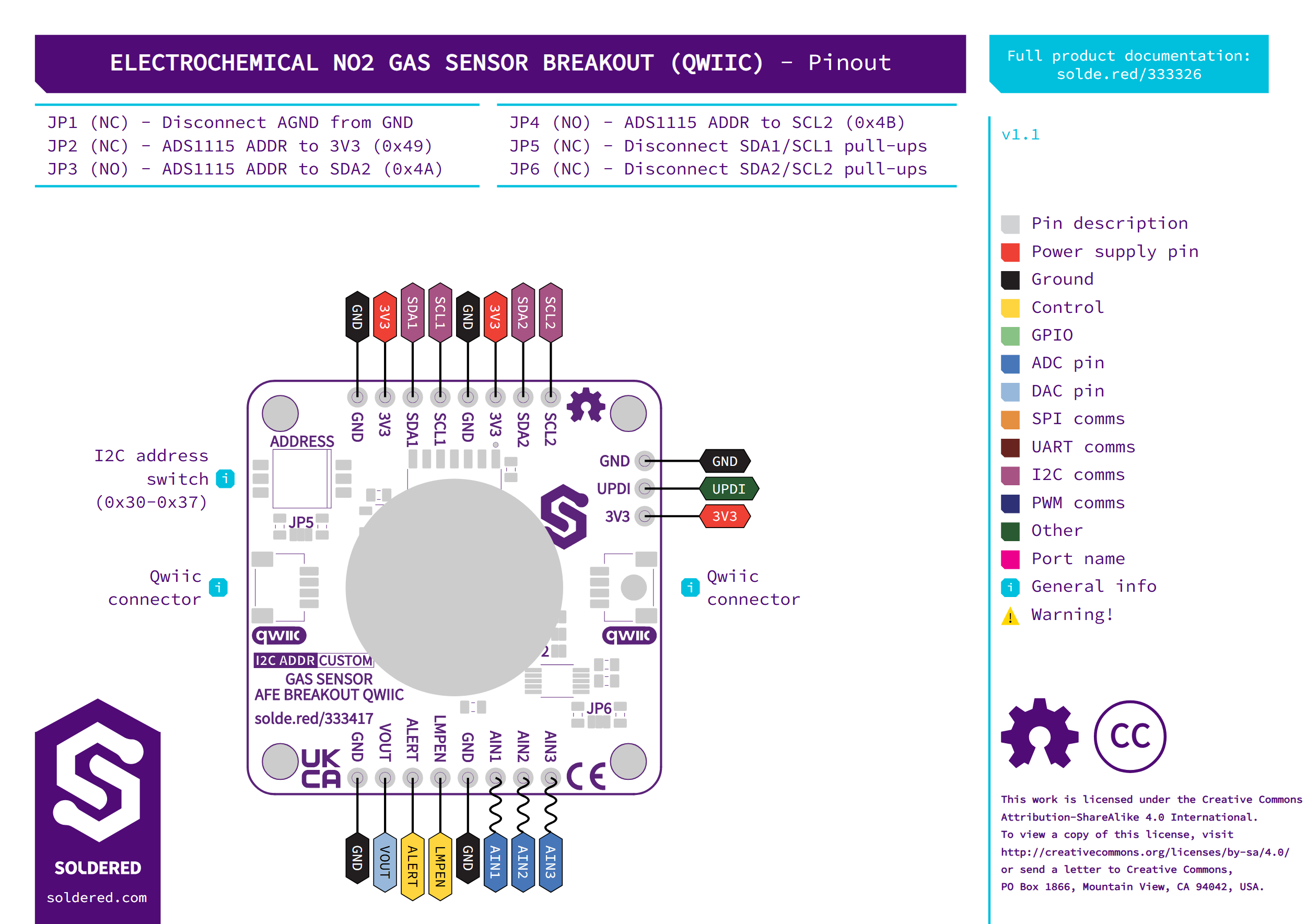
The board has two I2C buses. SDA1/SCL1 is the bus your controller uses: it
is wired to both Qwiic connectors and to the ATtiny404. SDA2/SCL2 is the
board's own bus, where the ATtiny404 talks to the LMP91000 (at 0x48) and the
ADS1115 (at 0x49).
| Pin marking | Pin name | Description |
|---|---|---|
GND | Ground | Ground. Every GND pin is the same ground. |
3V3 | 3.3 V supply | The board's only supply, shared with the Qwiic connectors. 3.3 V only. |
SDA1, SCL1 | Main I2C bus | Same bus as the Qwiic connectors. Connect your controller here when you do not use Qwiic. |
SDA2, SCL2 | Internal I2C bus | The bus between the ATtiny404, the LMP91000 and the ADS1115. |
VOUT | Analog output | The LMP91000's output voltage from the gas cell, which the ADS1115 also reads on its AIN0 input. |
ALERT | ADC alert | The ADS1115's ALERT/RDY pin, with a 10 kΩ pull-up to 3V3. |
LMPEN | Front-end enable | The LMP91000's module-enable input, also wired to the ATtiny404. |
AIN1, AIN2, AIN3 | Analog inputs | The ADS1115's other three inputs. The ADS1115 sits on the internal bus that the ATtiny404 runs, and the ElectrochemicalGasSensor class in both libraries reads only the gas channel, so the libraries do not read these inputs. |
UPDI | Programming | The ATtiny404's programming pin, on the three-pin header with GND and 3V3 at the right edge. |
Voltage and logic levels
| Connection | Supported voltage | Notes |
|---|---|---|
3V3 and the Qwiic connectors | 3.3 V | No regulator. Do not apply 5 V. |
SDA1, SCL1, SDA2, SCL2 | 3.3 V logic | 10 kΩ pull-ups to 3V3 on each bus. |
The board has no level shifter, so its I2C lines are pulled up to 3.3 V.
Dimensions
The board measures 38 x 38 mm and has a 3.2 mm mounting hole in each corner. The gas cell sits on the underside.
Jumpers
The ADDRESS switches set the board's I2C address from 0x30 to 0x37; the
board ships at 0x30.
| Jumper | Default | Function |
|---|---|---|
| ADDRESS switches 1 to 3 | Address 0x30 | Set the board's I2C address on the Qwiic bus, 0x30 to 0x37. |
JP5 | Closed | Connects the 10 kΩ pull-ups on SDA1/SCL1. Cut it to disconnect them. |
JP6 | Closed | Connects the 10 kΩ pull-ups on SDA2/SCL2. Cut it to disconnect them. |
JP2 to JP4 | JP2 closed, JP3 and JP4 open | ADS1115 address on the internal bus: JP2 ties ADDR to 3V3 (0x49, as shipped), JP3 to SDA2 (0x4A), JP4 to SCL2 (0x4B). Keep JP2 closed when you read the board through the ATtiny404: the libraries never send it the ADC address, and it is not confirmed that its factory firmware follows a move to 0x4A or 0x4B. |
JP1 | Closed | Connects the front end's analog ground to GND. Cut it to separate them. |
Close only one of JP2, JP3 and JP4. All three join the ADS1115 ADDR pin,
so two closed jumpers tie their other sides together: JP2 with JP3 or
JP4 connects 3V3 straight to SDA2 or SCL2, and JP3 with JP4
connects SDA2 to SCL2.