Hardware Details
The SGX-4OX-ROHS oxygen cell sits on the underside of the board. On the top, an LMP91000 analog front end biases the cell and turns its current into a voltage, an ADS1115 16-bit ADC converts that voltage, and an ATtiny404 talks to both chips over the board's own I2C bus. Your controller sees one I2C device: the ATtiny404, at 0x30 by default.
Key specifications
| Specification | Value |
|---|---|
| MCU | |
| Bridge MCU | Microchip ATtiny404, factory firmware |
| Interface | |
| Interface | I2C; analog output VOUT and analog inputs AIN1 to AIN3 on the header |
| Qwiic compatible | Yes, 2 connectors |
| Default I2C address | 0x30 |
| I2C address changeable | Yes, 0x30 to 0x37 with the ADDRESS switch |
| Breadboard compatible | No |
| Power | |
| Supply voltage | 3.3 V (no regulator) |
| Logic level | 3.3 V only |
| Other | |
| Analog front end | Texas Instruments LMP91000 |
| ADC | Texas Instruments ADS1115, 16-bit |
| Gas cell | SGX-4OX-ROHS, electrochemical, oxygen (O2) |
| Measurement range | 0 to 25 % vol O2; maximum overload 30% O2 |
| Response time | T90 under 10 s |
| Repeatability | < ±2% SO2 equivalent |
| Cell output | Logarithmic, S = K ln(1/(1-C)); 0.1 ± 0.03 mA in air |
| Cell bias | −600 mV |
| Operating conditions | −40 to 60 °C, 15 to 90% RH |
| Expected cell life | Over 60 months in air |
| Dimensions | 38 x 38 mm |
After power-up the cell can take up to 15 minutes to settle.
Pinout
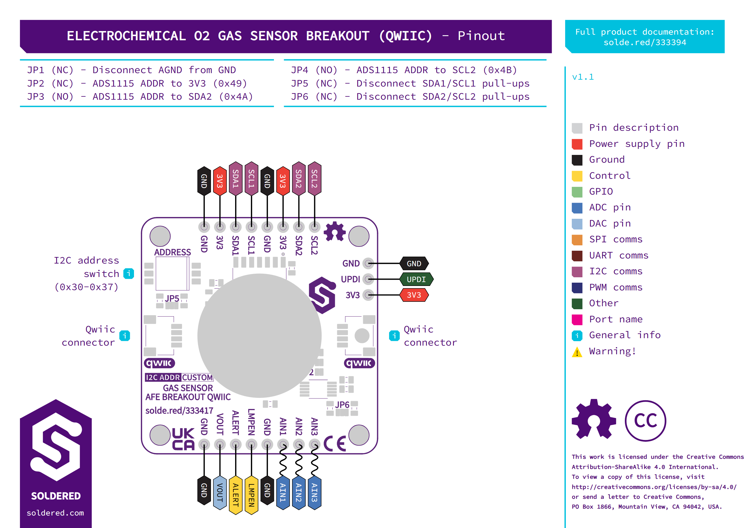
| Pin marking | Pin name | Description |
|---|---|---|
| Qwiic (x2) | 3V3, SDA1, SCL1, GND | Power and the controller's I2C bus. Either connector works; both carry the same four lines. |
3V3 | 3.3 V supply | The board's only supply. Every 3V3 pin and both Qwiic connectors are joined. |
GND | Ground | All GND pins are joined. |
SDA1, SCL1 | Controller I2C bus | The bus your controller uses to reach the ATtiny404, the same lines as the Qwiic connectors. 10 kΩ pull-ups to 3V3. |
SDA2, SCL2 | Internal I2C bus | The bus between the ATtiny404, the LMP91000 (0x48) and the ADS1115 (0x49 by default). 10 kΩ pull-ups to 3V3. |
VOUT | Front end output | The LMP91000's analog output voltage, which the ADS1115 converts on its AIN0 input. |
ALERT | ADC alert | The ADS1115's ALERT pin, also wired to the ATtiny404. |
LMPEN | Front end enable | The LMP91000's enable input. A 10 kΩ resistor holds it at GND, and it is also wired to the ATtiny404. You do not need to wire it. |
AIN1, AIN2, AIN3 | ADC inputs | The ADS1115's other three inputs, free for your own analog signals. |
UPDI | Programming | With the 3V3 and GND beside it, the ATtiny404's UPDI programming connection. |
Voltage and logic levels
| Connection | Supported voltage | Notes |
|---|---|---|
3V3 pins and Qwiic connectors | 3.3 V | No regulator: what you feed in is what the chips get. |
SDA1, SCL1, SDA2, SCL2 | 3.3 V logic | Pulled up to 3V3 through 10 kΩ. |
Do not connect 5 V to the board. It is 3.3 V only and has no regulator or level shifter.
The board also has a 2.5 V reference for the front end; the libraries' presets
all select it (REF_EXTERNAL). A footprint for an external gain resistor on the
front end is left unfitted; the libraries'
TIA_GAIN_EXTERNAL setting and setCustomTiaGain() function are for that
case.
Dimensions
The board measures 38 x 38 mm and has four 3.2 mm mounting holes, one in each corner. The gas cell is mounted on the underside.
Jumpers
| Jumper | Default | Function |
|---|---|---|
| ADDRESS switch (3 positions) | 0x30 | Sets the board's I2C address from 0x30 to 0x37. Each position connects one address line of the ATtiny404 to GND when on. |
| JP1 | Closed | Connects the front end's analog ground (AGND) to GND. Cut it to separate them. |
| JP2 to JP4 | JP2 closed, JP3 and JP4 open | ADS1115 address on the internal bus: JP2 ties ADDR to 3V3 (0x49), JP3 to SDA2 (0x4A), JP4 to SCL2 (0x4B). |
| JP5 | Closed | Connects the 10 kΩ pull-ups on SDA1 and SCL1. Cut it to disconnect them. |
| JP6 | Closed | Connects the 10 kΩ pull-ups on SDA2 and SCL2. Cut it to disconnect them. |
Close only one of JP2, JP3 and JP4 at a time. All three join the ADS1115's
ADDR pin: closing JP3 or JP4 while JP2 is still closed connects SDA2 or
SCL2 to 3V3, and closing JP3 and JP4 together connects SDA2 to SCL2.