Hardware Details
NULA Node RP2040 brings out 24 of the RP2040's GPIO pins across two 15-pin headers, plus a 3-pin SWD (serial wire debug) header for a hardware debugger. Three GPIO pins double as 12-bit ADC (analog-to-digital converter) inputs. A Qwiic connector carries I2C separately from the headers, so you can plug in a sensor without using up header pins.
Pinout
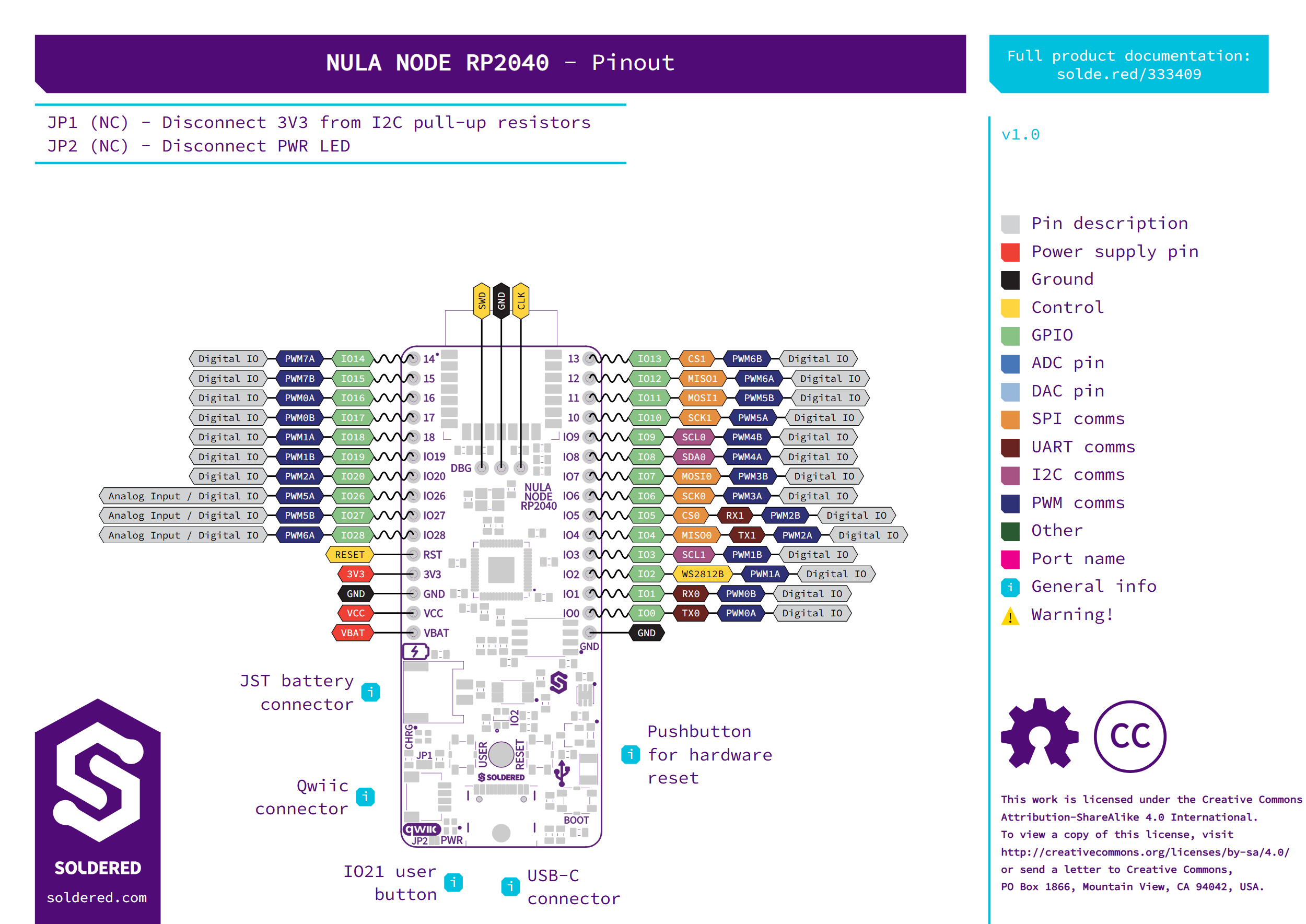
Pin details
| Pin marking | Pin name | Description |
|---|---|---|
| 14 | IO14 | Digital I/O, PWM7A |
| 15 | IO15 | Digital I/O, PWM7B |
| 16 | IO16 | Digital I/O, PWM0A |
| 17 | IO17 | Digital I/O, PWM0B |
| 18 | IO18 | Digital I/O, PWM1A |
| IO19 | IO19 | Digital I/O, PWM1B |
| IO20 | IO20 | Digital I/O, PWM2A |
| IO26 | IO26 | Analog input (ADC) or digital I/O, PWM5A |
| IO27 | IO27 | Analog input (ADC) or digital I/O, PWM5B |
| IO28 | IO28 | Analog input (ADC) or digital I/O, PWM6A |
| RST | RESET | Pull low to reset the board |
| 3V3 | 3V3 | 3.3 V power output |
| GND (left header) | Ground | Ground reference |
| VCC | VCC | Power input, 3.3 V to 5 V |
| VBAT | VBAT | 3.7 V Li-Ion battery input, wired to the onboard charger |
| 13 | IO13 | Digital I/O, SPI1 chip select (CS1), PWM6B |
| 12 | IO12 | Digital I/O, SPI1 MISO (MISO1), PWM6A |
| 11 | IO11 | Digital I/O, SPI1 MOSI (MOSI1), PWM5B |
| 10 | IO10 | Digital I/O, SPI1 clock (SCK1), PWM5A |
| IO9 | IO9 | Digital I/O, I2C0 clock (SCL0), PWM4B |
| IO8 | IO8 | Digital I/O, I2C0 data (SDA0), PWM4A |
| IO7 | IO7 | Digital I/O, SPI0 MOSI (MOSI0), PWM3B |
| IO6 | IO6 | Digital I/O, SPI0 clock (SCK0), PWM3A |
| IO5 | IO5 | Digital I/O, SPI0 chip select (CS0), UART1 RX (RX1), PWM2B |
| IO4 | IO4 | Digital I/O, SPI0 MISO (MISO0), UART1 TX (TX1), PWM2A |
| IO3 | IO3 | Digital I/O, I2C1 clock (SCL1), PWM1B |
| IO2 | IO2 | Digital I/O, also drives the onboard WS2812B addressable LED, PWM1A |
| IO1 | IO1 | Digital I/O, UART0 RX (RX0), PWM0B |
| IO0 | IO0 | Digital I/O, UART0 TX (TX0), PWM0A |
| GND (right header) | Ground | Ground reference |
| SWD | SWD | Serial wire debug data, for a hardware debugger |
| GND (debug header) | Ground | Ground reference |
| CLK | CLK | Serial wire debug clock, for a hardware debugger |
The onboard USER button is wired to IO21, which isn't broken out to either header. The RESET button and the RST header pin both reset the board in hardware.
Power supply
Power the board over USB-C, which also handles programming and the serial connection; a 500 mA fuse protects the input. A 2-pin JST connector and an onboard Li-Ion charger let you run it from a 3.7 V Li-Ion battery instead, and the board switches between USB and battery power on its own, so unplugging the cable doesn't reset your project. VCC accepts 3.3 V to 5 V. Logic throughout the board is 3.3 V.
Dimensions
- Board size: 26 x 65 mm
- Header spacing: rows 22.86 mm (0.9 in) apart, breadboard-friendly; header pins are included but unsoldered
Jumpers
| Jumper | Default | Function |
|---|---|---|
| JP1 | Connected (closed) | Cut to disconnect 3.3 V from the I2C pull-up resistors |
| JP2 | Connected (closed) | Cut to disconnect the power LED |