Hardware Details
The PCA9685 does the actual PWM generation. This board wires it up with two Qwiic connectors, a 6-pin header, a screw terminal for servo power, six solder jumpers that set the I2C address, and a seventh that controls the I2C pull-up resistors.
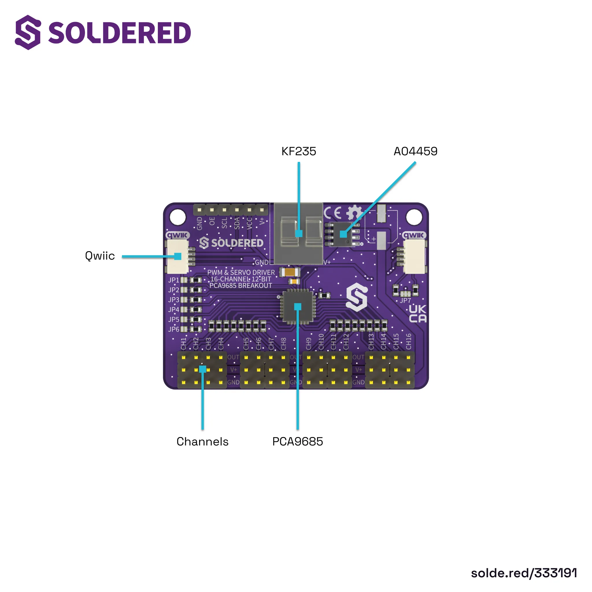
The servo-power screw terminal is a KF235. The small IC next to it, marked A04459, is the AO4459 P-channel MOSFET that protects the board if the servo supply is wired backwards.
Key specifications
| Specification | Value |
|---|---|
| Interface | |
| Interface | I2C (control), PWM (16 outputs) |
| Qwiic connectors | 2 |
| Default I2C address | 0x40 |
| Address range | 0x40 to 0x7F, set with six solder jumpers |
| Channels | 16, individually programmable |
| Resolution | 12-bit, 4096 steps per channel |
| PWM frequency | 24 Hz to 1526 Hz, shared by all channels. 200 Hz at IC power-on; the Soldered libraries set 50 Hz on init |
| Power | |
| Logic supply | 3.3 V, 6 mA typical / 10 mA maximum |
| Output drive | 25 mA sink, 10 mA source per channel at 5 V; 400 mA total for the package |
| Other | |
| Driver IC | PCA9685 (NXP), part PCA9685BS,118 |
| Dimensions | 54 x 38 x 7.2 mm |
| Mounting holes | 2 x 3.2 mm |
| Operating temperature | -40 °C to +85 °C |
Pinout
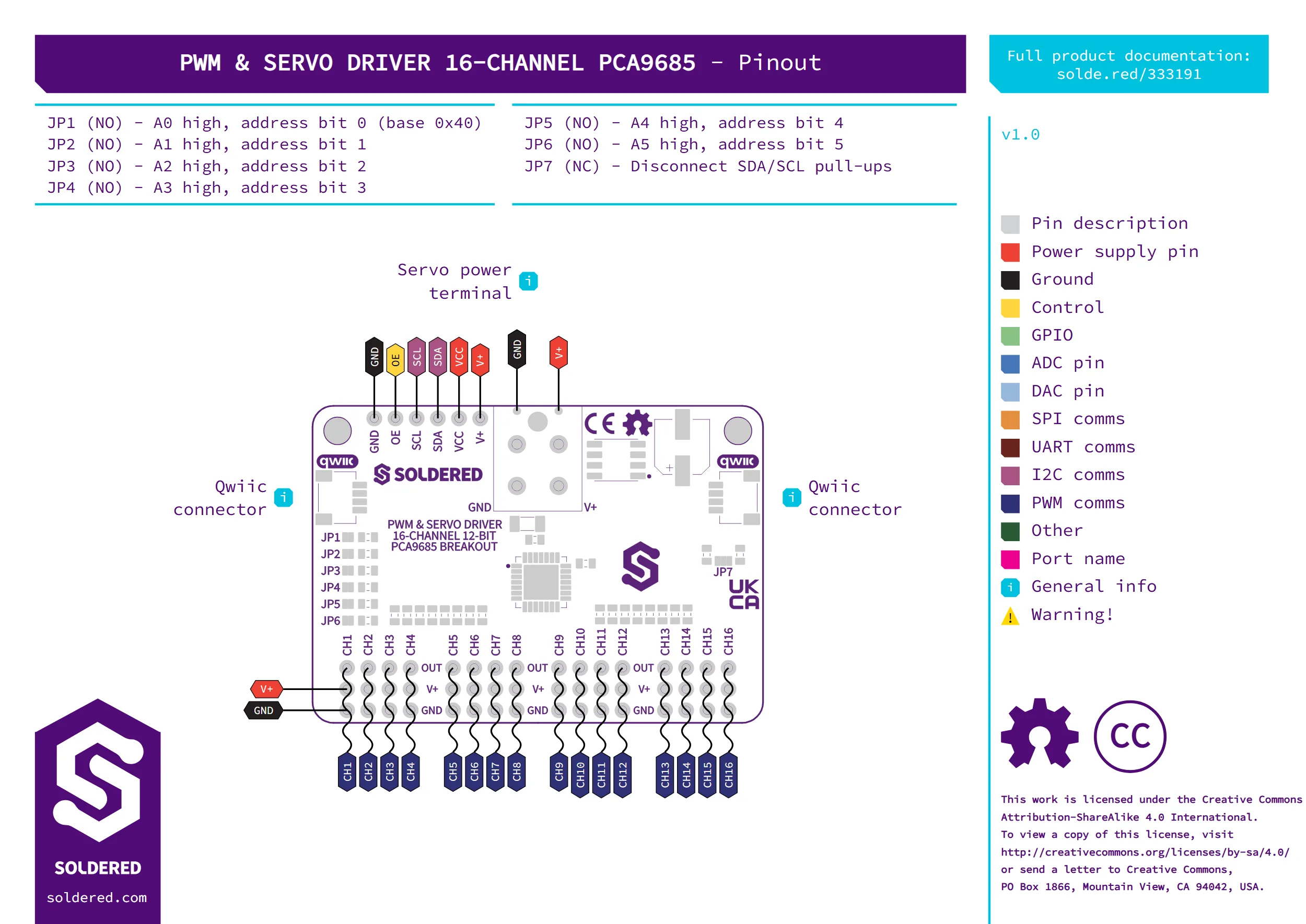
| Pin marking | Pin name | Description |
|---|---|---|
| GND (header) | Logic ground | Ground reference for the header connection. |
| OE | Output enable | Active low. Pulled low on board, so all 16 outputs are enabled by default. Drive it high to disable every output at once. |
| SCL | I2C clock | Connect to your controller's I2C clock line. Also carried by the Qwiic connectors. |
| SDA | I2C data | Connect to your controller's I2C data line. Also carried by the Qwiic connectors. |
| VCC | Logic supply | 3.3 V supply for the PCA9685 IC. Also carried by the Qwiic connectors. |
| V+ (header) | Servo power, header | Same rail as the screw terminal's V+. Lets you power servos from the header instead of the screw terminal. |
| V+ (screw terminal) | Servo power input | 5 mm screw terminal. Powers the servo/PWM loads on all 16 channels, separate from the logic supply. |
| GND (screw terminal) | Servo power ground | Ground return for the servo power supply. |
| qwiic (x2) | Qwiic connectors | Plug-and-play I2C, carrying SCL, SDA, 3.3 V and GND. Either connector works; the other is free for chaining another Qwiic board. |
| CH1-CH16 OUT | Channel PWM output | One PWM signal per channel, numbered 0 to 15 in the library API. |
| CH1-CH16 V+ | Channel power | The servo power rail, broken out per channel. |
| CH1-CH16 GND | Channel ground | Ground, broken out per channel. |
| JP1-JP6 | Address-select jumpers | Binary address bits A0 (LSB, JP1) to A5 (JP6). All open (the default) gives address 0x40; closing jumpers adds their bit value, up to 0x7F with all six closed. See the bit-weight table below. |
| JP7 | I2C pull-up jumper | Closed by default, connecting two 10 kΩ pull-ups to SDA and SCL. Cut it to disconnect them. |
Voltage and logic levels
| Connection | Supported voltage | Notes |
|---|---|---|
| Logic (VCC) | 3.3 V only | Not documented as 5 V tolerant. Power the header from a 3.3 V rail if not using Qwiic. |
The Qwiic connector carries 3.3 V logic power along with I2C, so a Qwiic-only connection powers the PCA9685's logic side automatically. Servo power still needs its own supply on the screw terminal or the header's V+ pad; it is not carried over Qwiic.
Dimensions
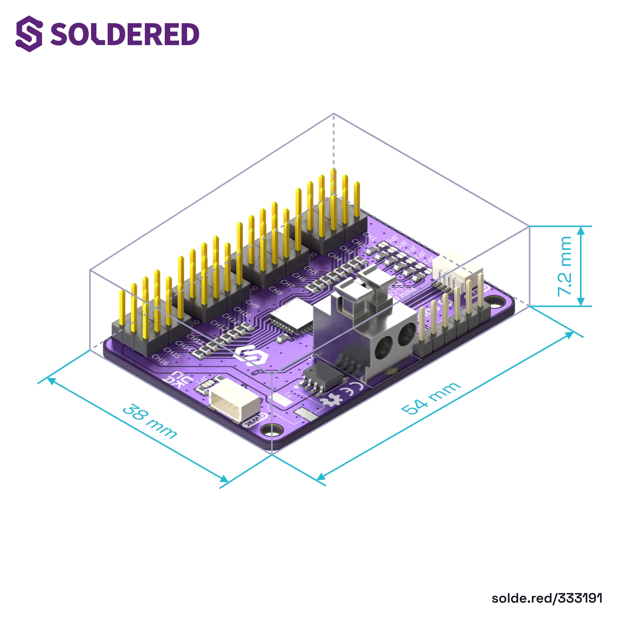
54 x 38 mm, 7.2 mm tall, with 2 mounting holes of 3.2 mm diameter.
Jumpers
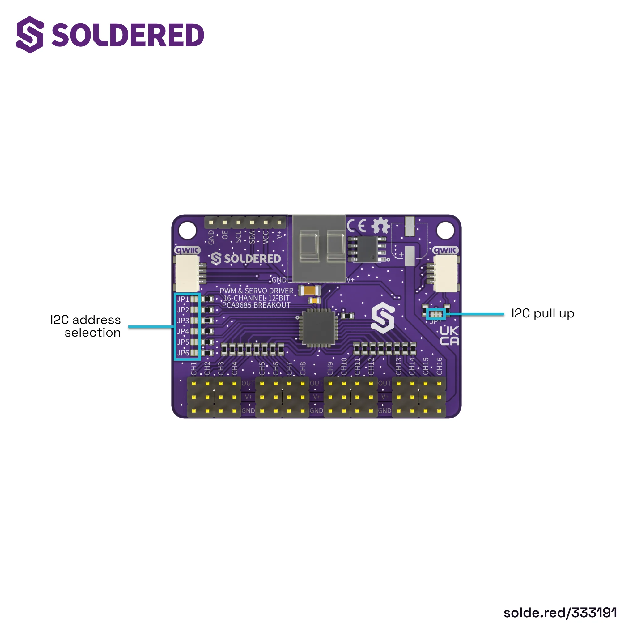
| Jumper | Default | Function |
|---|---|---|
| JP1 to JP6 | Open | I2C address selection. Each jumper is one address bit, JP1 the LSB (A0, +1) through JP6 (A5, +32). Close a combination to add their values to 0x40. |
| JP7 | Closed | I2C pull-up jumper. Connects two 10 kΩ resistors from VCC to SDA and SCL. Cut it to disconnect the pull-ups. |
Two address settings must not be used. 0x70 (JP5 and JP6 closed, the rest
open) is the PCA9685's LED All Call address: it is active from power-up,
begin() keeps it on, and every PCA9685 on the bus answers it. 0x7C to
0x7F (JP3 to JP6 closed, with or without JP1 and JP2) are reserved I2C
addresses. Both are listed as reserved in section 7.1 of the
PCA9685 datasheet.
All six address jumpers open gives the default address, 0x40. Closing a combination of JP1 to JP6 adds their bit values, so any address from 0x40 to 0x7F is reachable; all six closed gives 0x40 + 63 = 0x7F.
For example, to set the address to 0x45 (0x40 + 5, or binary 000101), close
JP1 (A0, +1) and JP3 (A2, +4), and leave JP2, JP4, JP5 and JP6 open.