Hardware Details
The LTC4331 from Analog Devices does the extending. It turns the I2C bus into a differential signal on a twisted pair, so the same transparent bus can run across an Ethernet cable. This board adds a Qwiic connector, an RJ45 jack, two 6-pin headers for the control and status pins, and solder jumpers for the link speed, the control address and the pull-up resistors.
Key specifications
| Specification | Value |
|---|---|
| Interface | |
| Interface | I2C (Qwiic) |
| Qwiic compatible | Yes |
| Default I2C address | 0x77 (the LTC4331's own control device) |
| I2C address changeable | Yes, 0x3C to 0x3F and 0x74 to 0x77 with the A1 and A2 jumpers, or disabled |
| Breadboard compatible | Yes |
| Link | Differential over twisted-pair cable, RJ45 jack |
| Link speed | 12.5 kHz to 1 MHz, set with the SPEED1 and SPEED2 jumpers (default 1 MHz) |
| Maximum cable length | 30 m at 1 MHz up to over 1200 m at 100 kHz and below |
| Mode | Local by default, remote when the REMOTE pin is tied to 3.3 V |
| Pull-up resistors | 10 kΩ on SDA and SCL, disconnectable with a solder jumper |
| Power | |
| Supply voltage | 3.3 V |
| Logic level | 3.3 V only |
| Operating current | 65 mA |
| Sleep current | 40 µA |
| Protection | ESD |
| Other | |
| IC | LTC4331 (Analog Devices) |
| Connectors | One Qwiic, one RJ45, two 6-pin 2.54 mm headers |
| Dimensions | 38 × 22 mm |
| Mounting | Two 3.2 mm holes |
| Operating temperature | −40 °C to 85 °C (LTC4331I) |
Pinout
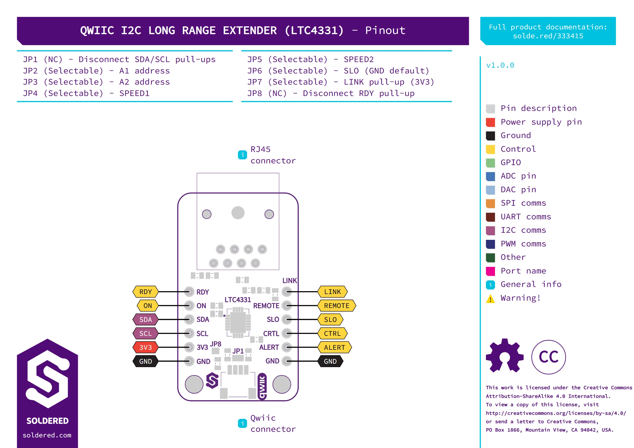
The left header (K2) carries the I2C side. The right header (K3) carries the control and status pins of the link. Pins are listed top to bottom as drawn above.
| Pin marking | Pin name | Description |
|---|---|---|
RDY | RDY | I2C ready status, open-drain. Goes low once the board's I2C interface has joined the bus. Only valid on the local side. |
ON | ON | Enable input. Keep it high for operation. Low puts the LTC4331 into low-power mode, with its outputs disabled. |
SDA | SDA | I2C data. |
SCL | SCL | I2C clock. |
3V3 | 3V3 | 3.3 V supply. |
GND | GND | Ground. |
LINK | LINK | Link status, open-drain. Goes low once the link to the second board is established. Only valid when a local board is connected to a remote board. |
REMOTE | REMOTE | Mode select. Left unconnected it reads low (local side). Tie it to 3.3 V on the far board to make it the remote side. |
SLO | SLO | Link slow mode. Low limits the slew rate of the link transmitter, which only matters at the two slowest link speeds. |
CRTL | CTRL | One digital signal passed from the local board to the remote board. The silkscreen prints it as CRTL. |
ALERT | ALERT | Interrupt, passed back from the remote side to the local side. |
GND | GND | Ground. |
The Qwiic connector (K4) carries SCL, SDA, 3V3 and GND.
The RJ45 jack (K1) carries the differential link:
| RJ45 pin | Signal |
|---|---|
| 1 | DIFF+ |
| 2 | DIFF- |
| 5 | GND |
| 6 | 3V3 |
| 3, 4, 7, 8 | Not connected |
Voltage and logic levels
| Connection | Supported voltage | Notes |
|---|---|---|
| Qwiic connector and headers | 3.3 V | Supply and logic level. The board is 3.3 V only. |
| RJ45 jack | 3.3 V | Carries 3V3 and GND alongside the differential pair. |
This board is 3.3 V only, for both supply and I2C logic. Do not connect a 5 V supply or 5 V logic.
Dimensions
The board is 38 × 22 mm, with two 3.2 mm mounting holes.
Jumpers
JP2 to JP7 are on the back of the board. The others are on the front.
| Jumper | Default | Function |
|---|---|---|
| JP1 | Closed | Connects 3.3 V to the SDA and SCL pull-up resistors (10 kΩ each). Cut it to disconnect them. |
| JP2, JP3 | 3.3 V | I2C address of the LTC4331's control device. JP2 sets A1 and JP3 sets A2. Each one is high (3.3 V, default), low (GND) or open. See the address table below. |
| JP4, JP5 | GND | Link speed. JP4 sets SPEED1 and JP5 sets SPEED2. Each one is low (GND, default), high (3.3 V) or open. See the speed table below. |
| JP6 | GND | SLO level. Low (GND, default) limits the link slew rate. The other position connects SLO to 3.3 V through a pull-up. |
| JP7 | 3.3 V pull-up | LINK pin. The default connects LINK to a pull-up resistor so the status can be read. The other position connects LINK to GND. |
| JP8 | Closed | Connects the pull-up resistor on RDY. Cut it to disconnect it. |
Do not leave JP6 open. The LTC4331 datasheet says the SLO pin must not
be allowed to float, so keep JP6 on GND or 3.3 V.
To change a 3-pad jumper, cut the trace between the two pads that are joined, then bridge the pair you want with solder. To leave a pin open, cut the trace and bridge nothing.
I2C address (JP2 and JP3)
The LTC4331 has an internal I2C device for status and configuration. The address
is set by A1 and A2. None of these addresses is reserved by the I2C
specification.
| A1 (JP2) | A2 (JP3) | Address |
|---|---|---|
| High | High | 0x77 (default) |
| Open | High | 0x74 |
| Low | High | 0x76 |
| High | Open | 0x75 |
| High | Low | 0x3F |
| Open | Low | 0x3C |
| Low | Open | 0x3D |
| Low | Low | 0x3E |
| Open | Open | Internal device disabled |
Link speed (JP4 and JP5)
| SPEED1 (JP4) | SPEED2 (JP5) | Link rate | Maximum cable length |
|---|---|---|---|
| Low | Low | 1 MHz | 30 m (default) |
| Open | Low | 500 kHz | 60 m |
| High | Low | 250 kHz | 200 m |
| Low | Open | 125 kHz | 600 m |
| Low | High | 100 kHz | 1200 m |
| High | Open | 63 kHz | Over 1200 m |
| Open | Open | 31 kHz | Over 1200 m |
| Open | High | 20 kHz | Over 1200 m |
| High | High | 12.5 kHz | Over 1200 m |
The maximum lengths come from the LTC4331 datasheet, measured with Cat5E Ethernet cable in a lab. The length you reach depends on your cable and surroundings.