Hardware Details
The board is 64 WS2812B LEDs and little else. Each WS2812B has its own control circuit and RGB chip in one 5050 package: it keeps the first 24 bits of colour data it receives and passes the rest on, reshaped, to the next LED. That is why one data line drives the whole grid.
- LEDs: 64 WS2812B in 8 rows of 8, 10 mm apart, each with its own 100 nF decoupling capacitor.
- Data path:
DINreaches the first LED, at the top left, through a 100 Ω series resistor. The data then runs in a serpentine, the first row left to right, the next right to left, and so on down the grid, and leaves the last LED onDOUT. - Power:
VCCgoes straight to every LED. There is no regulator and no level shifter on the board.
Key specifications
| Specification | Value |
|---|---|
| Interface | |
| Interface | Single-wire digital data: DIN in, DOUT out |
| Data rate | 800 kbps, 24 bits per LED, green-red-blue order |
| Qwiic compatible | No |
| Breadboard compatible | Yes, header pins included (unsoldered) |
| Power | |
| Supply voltage | 5 V on VCC, 4.5 V to 5.3 V |
| Logic level | 5 V only; DIN high from 0.7 x VCC, low up to 0.3 x VCC |
| Operating current | 3840 mA (no conditions stated) |
| Other | |
| LED IC | WS2812B (5050 package), 64 pieces |
| Layout | 8 x 8, 10 mm pitch |
| Colour depth | 256 levels per colour, 16777216 colours |
| Data input | 100 Ω series resistor on DIN |
| Decoupling | 100 nF per LED |
| Dimensions | 80 x 80 mm |
| Mounting holes | 4 x 3.2 mm |
Pinout
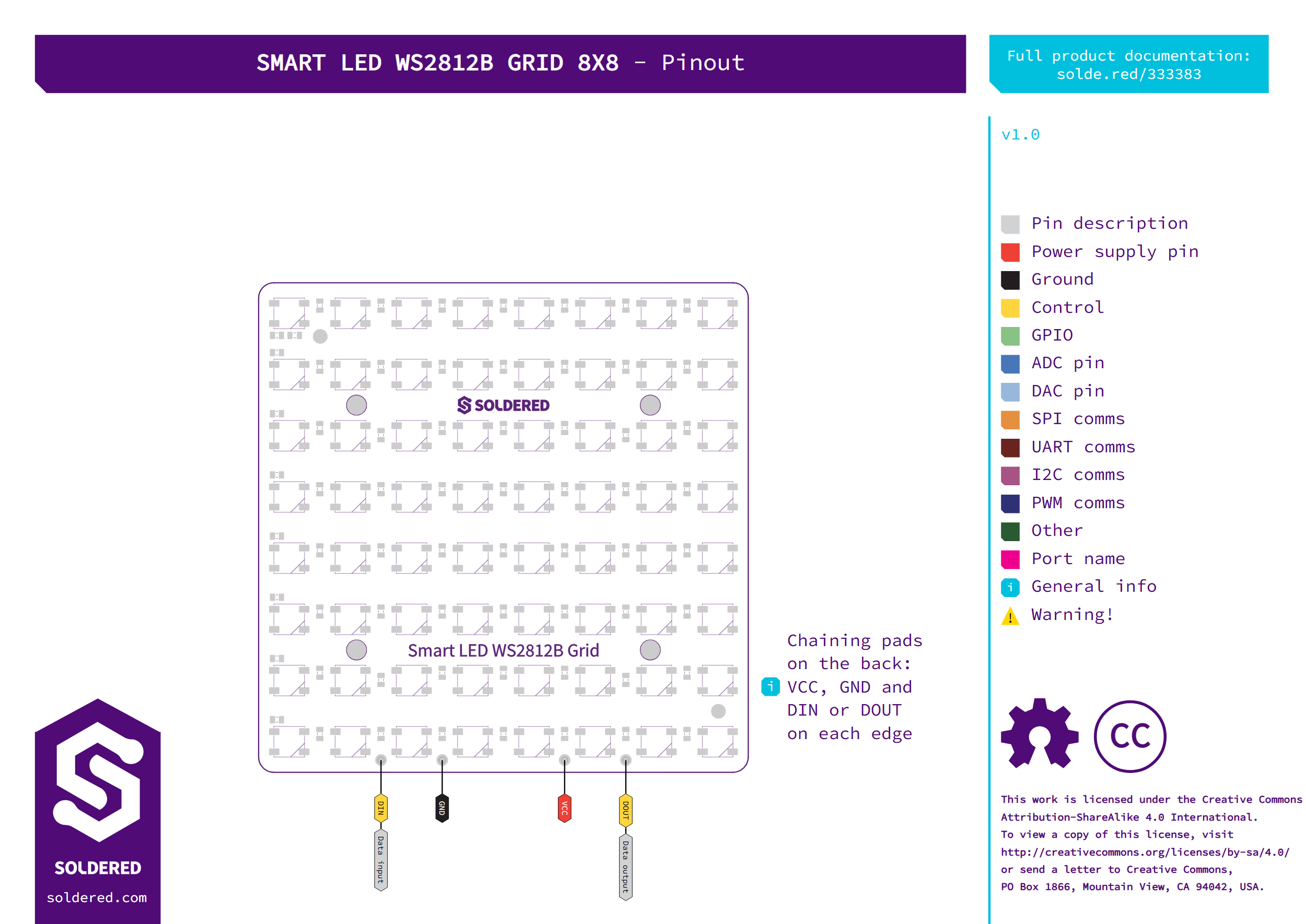
| Pin marking | Pin name | Description |
|---|---|---|
| DIN | Data in | Data from your controller to the first LED, through the 100 Ω series resistor. |
| GND | Ground | Common ground for power and data. |
| VCC | 5 V supply | Powers every LED directly, 4.5 V to 5.3 V. |
| DOUT | Data out | Data out of the last LED. Connect it to DIN of the next grid to chain grids. |
| Edge pads | VCC, GND, DIN or DOUT | Solder pads on every edge that line up with the neighbouring grid, for joining grids into a panel. |
To build a panel from several grids, connect DOUT of one grid to DIN of the
next. The libraries number the grids column first: all grids of the first
column from top to bottom, then the next column. Connect DOUT of the last grid
in each column to DIN of the first grid in the next column.
Each grid powers its LEDs only from its own VCC, so the data link alone is not
enough. Join VCC and GND between the grids too, with the edge pads or with
wires, so that every grid gets 5 V and shares its ground with the data line.
Voltage and logic levels
| Connection | Supported voltage | Notes |
|---|---|---|
VCC | 5 V (4.5 V to 5.3 V) | Feeds all 64 LEDs directly. 5.3 V is the WS2812B's absolute maximum supply. |
DIN | 5 V logic | High from 0.7 x VCC, which is 3.5 V at a 5 V supply; low up to 0.3 x VCC. No level shifter on the board. |
Keep VCC at or below 5.3 V, the WS2812B's absolute maximum. A 3.3 V data
signal is below the 3.5 V the LEDs need to read a high at a 5 V supply, so
the grid is specified for a 5 V logic signal on DIN.
The library examples set the brightness to 40 out of 255 and say to keep it low to avoid excessive current draw.
Running the SetPixel example, the grid draws an estimated 80 mA from 5 V. This is a calculation, not a measurement. It takes the 3840 mA operating current as all 64 LEDs at full white: 60 mA per LED, or 20 mA per colour at 255. SetPixel lights nine colour channels at 40 out of 255 (one each for the red, green and blue pixels, three for each of the two white pixels), about 28 mA. For the LEDs' own idle draw it assumes about 0.6 mA per LED, which adds about 38 mA; the datasheet gives no idle figure, so this part is our assumption. That makes about 66 mA, and about 20 % on top for calculation error gives about 80 mA.
Dimensions
The board measures 80 x 80 mm. The LEDs sit 10 mm apart, and the centres of the outer LEDs are 5 mm from the board edges. Four mounting holes, each 3.2 mm in diameter, let you screw the board down. Their centres form a 48 x 40 mm rectangle centred on the board: 48 mm apart along the LED rows and 40 mm apart along the columns.
Jumpers
The board has no configuration solder jumpers. The three-pad groups on the edges are the chaining pads described under Pinout.