Hardware Details
The board carries the Bosch BMA400 accelerometer, two Qwiic connectors, two
4-pin 2.54 mm headers and three solder jumpers. The 3V3 pin powers the
BMA400 directly: there is no regulator and no level shifter.
Key specifications
| Specification | Value |
|---|---|
| Interface | |
| Interface | I2C; INT1 and INT2 interrupt outputs |
| Qwiic compatible | Yes, 2x Qwiic connector |
| Default I2C address | 0x14 |
| I2C address changeable | Yes, 0x15 with the address jumper or the ADDR pin |
| Breadboard compatible | Yes, 2x 4-pin 2.54 mm header (supplied unsoldered) |
| Measurement | |
| Measurement types | Acceleration, 3 axes, 12-bit |
| Measurement range | ±2 g, ±4 g, ±8 g, ±16 g (selectable); ODR 12.5 to 800 Hz in normal mode, 25 Hz in low-power mode |
| Measurement accuracy | Zero-g offset 50 mg typ. at ±4 g; sensitivity 1024 LSB/g at ±2 g; noise density 180 µg/√Hz (X, Y), 240 µg/√Hz (Z), normal mode OSR=3, ±4 g, 25 °C |
| Power | |
| Supply voltage | 1.72 V to 3.6 V on 3V3 |
| Logic level | Same as the supply on 3V3; not 5 V tolerant |
| Operating current | 14.5 µA typical, normal mode, OSR=3 (3.5 µA at OSR=0) |
| Low-power mode current | 850 nA typical at 25 Hz, OSR=0 |
| Sleep current | 160 nA typical |
| Other | |
| IC part number | Bosch BMA400 |
| Operating temperature | -40 to +85 °C |
| Dimensions | 22 x 22 mm |
| Mounting holes | 2x 3.2 mm |
The current figures are the BMA400's datasheet typical values at nominal supply and 25 °C.
Pinout
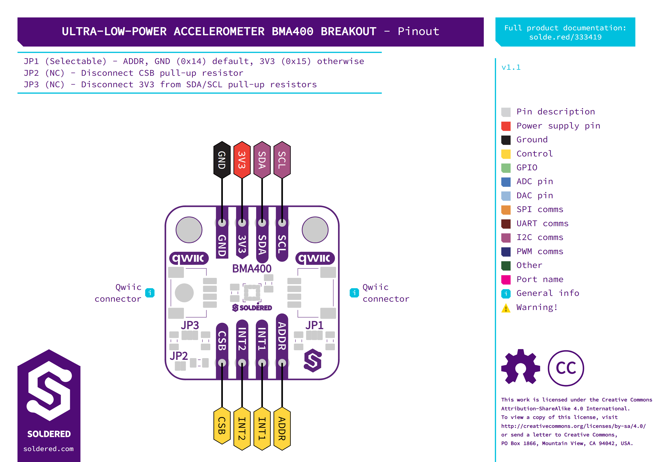
The board has two 4-pin headers. One carries power and I2C, the same four signals as the Qwiic connectors. The other carries the BMA400's address, interrupt and chip-select pins.
| Pin marking | Pin name | Description |
|---|---|---|
GND | Ground | Ground, shared with both Qwiic connectors. |
3V3 | Supply | 1.72 V to 3.6 V supply for the BMA400, shared with both Qwiic connectors. |
SDA | I2C data | I2C data line, 10 kΩ pull-up to 3V3 (see Jumpers). |
SCL | I2C clock | I2C clock line, 10 kΩ pull-up to 3V3 (see Jumpers). |
ADDR | Address select | The BMA400's address pin: low selects 0x14, high selects 0x15. Held low through 10 kΩ by default. |
INT1 | Interrupt 1 | Interrupt output 1. The library examples route their interrupts here. |
INT2 | Interrupt 2 | Interrupt output 2. |
CSB | Chip select | The BMA400's chip-select pin, held high through 10 kΩ by default for I2C. |
The libraries configure INT1 and INT2 as push-pull or open drain, active
high or low, with setInterruptPinMode() (Arduino) or
set_interrupt_pin_mode() (MicroPython). Leave an interrupt pin you do not use
unconnected, as the BMA400 datasheet asks.
Voltage and logic levels
| Connection | Supported voltage | Notes |
|---|---|---|
3V3 pin and Qwiic power | 1.72 V to 3.6 V | Feeds the BMA400's core and I/O supply directly, with no regulator. |
SDA, SCL | Same as 3V3 | Input low below 0.3 x the supply, input high above 0.7 x the supply. |
ADDR, CSB, INT1, INT2 | Same as 3V3 | No level shifter on the board. |
The BMA400's absolute maximum is 4 V on its supply and the supply plus 0.3 V
on any logic pin. Never connect 3V3 or any signal pin to 5 V, and use a
controller with 3.3 V logic.
Dimensions
The board is 22 x 22 mm. It has two 3.2 mm mounting holes along one edge, 16 mm apart centre to centre, each 3 mm in from the board edges. The headers use the standard 2.54 mm pitch.
Jumpers
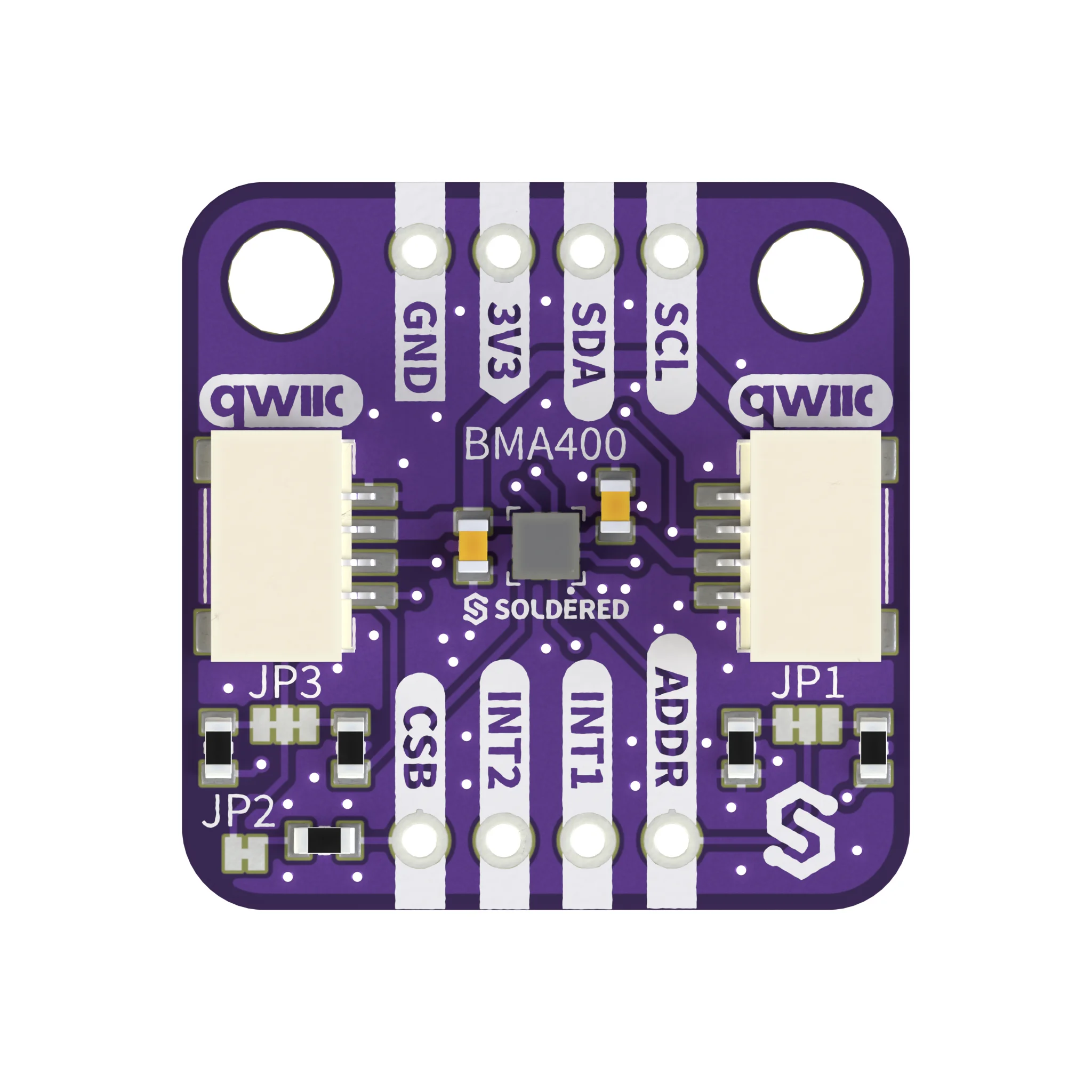
The jumpers are labelled on the board. With the GND, 3V3, SDA, SCL
header at the top, as in the photo, JP1 sits at the bottom right, under the
right-hand Qwiic connector and next to the ADDR pin. JP3 sits at the bottom
left, under the left-hand Qwiic connector, and JP2 sits below it in the
bottom-left corner, next to the CSB pin.
| Jumper | Default | Function |
|---|---|---|
JP1, address (3 pads) | Centre pad joined to the GND side: ADDR low, address 0x14 | Cut the trace to the GND side and bridge the centre pad to the other side with solder to pull ADDR high through 10 kΩ, for address 0x15. You can also leave the jumper as it is and drive the ADDR pin high from your controller. |
JP3, I2C pull-ups (3 pads) | Both sides joined: 10 kΩ pull-ups on SDA and SCL connected | Cut both traces to disconnect the pull-ups. |
JP2, CSB pull-up (2 pads) | Closed: CSB held high through 10 kΩ | Keep it closed. The BMA400 needs CSB high for I2C, and both libraries use I2C only. |
Never leave ADDR floating. The BMA400 needs a defined level on it in
I2C mode. Cutting JP1's default trace without bridging the
other side, with nothing driving the ADDR pin, leaves it floating.
Bridging all three pads of JP1 puts ADDR at about half the supply, between the
input-low and input-high limits, so the address is undefined.